www.austriamicrosystems.com/AS5130
Revision 1.12
17 - 41
AS5130
Datasheet - Detailed Description
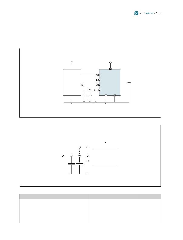
7.3 OTP Programming
For programming of the OTP, an additional voltage has to be applied to the pin PROG. It has to be buffered by a fast 100nF capacitor (ceramic)
and a 10礔 capacitor. The information to be programmed is set by command 25. The OTP bits 16 to 45 are used for AMS factory trimming and
cannot be overwritten.
Figure 12. OTP Programming Connection
Figure 13. External Circuitry for OTP Programming
Table 11. OTP Programming Parameters
Symbol
Parameter
Min
Max
Unit
Notes
VDD
Supply Voltage
5
5.5
V
GND
Ground Level
0
0
V
V_zapp
Programming Voltage
8
8.5
V
At pin PROG
T_zapp
Temperature
0
85
篊
f_clk
CLK Frequency
100
kHz
At pin DCLK
VDD
VSS
micro
controller
AS5130
100n
VSS
+5V
VDD
CS
VDD
DCLK
DIO
PROG
VSS
AS5130
C1
I/O
Output
Output
+
10礔
100n
8.0 - 8.5V
VDD
V
SUPPLY
PROG
GND
C1
C2
100nF 10礔
V
zapp
V
prog
PROM Cell
maximum
parasitic cable
inductance
L<50nH
发布紧急采购,3分钟左右您将得到回复。
相关PDF资料
AS5132-HSST-500
IC ENCODER ROTARY 20-SSOP
AS5134-ZSST-500
IC ENCODER RPTARY 20-SSOP
AS5140H-ASST
IC ENCODER ROTARY 10BIT 16-SSOP
AS5145B-HSST-500
IC ENCODER ROTARY MAGN 16-SSOP
AS5510-DWLT
IC ENCODER MAGNETIC LIN 6-WLCSP
ATS137-PL-B-B
IC HALL SENSOR SGL 25MA SIP-3L
ATS177-PG-B-B
IC HALL SENSOR LATCH 25MA SIP-3L
ATS617LSGTN-T
IC HALL EFFECT GEAR SENSOR 4SIP
相关代理商/技术参数
AS5130ASSU
制造商:AMS 功能描述:IC MAGNETIC ROTARY ENCODER 8BIT SSOP-16 制造商:AMS 功能描述:IC, MAGNETIC ROTARY ENCODER 8BIT SSOP-16; IC Function:Encoder IC; Brief Features:360 Contactless Angular Position Encoding, Two Digital 8-bit Absolute Output; Supply Voltage Min:3V; Supply Voltage Max:5.5V; No. of Pins:16 ;RoHS Compliant: Yes
AS5130-ASSU
功能描述:IC ENCODER ROTARY 8-BIT 16-SSOP RoHS:是 类别:传感器,转换器 >> 磁性 - 霍尔效应,数字式开关,线性,罗盘 (IC) 系列:- 标准包装:1 系列:- 传感范围:20mT ~ 80mT 类型:旋转 电源电压:4.5 V ~ 5.5 V 电流 - 电源:15mA 电流 - 输出(最大):- 输出类型:数字式,PWM,8.5 位串行 特点:可编程 工作温度:-40°C ~ 150°C 封装/外壳:20-SSOP(0.209",5.30mm 宽) 供应商设备封装:20-SSOP 包装:Digi-Reel® 其它名称:AS5132-HSST-500DKR
AS5130ATST
制造商:AMSCO 制造商全称:austriamicrosystems AG 功能描述:8 Bit Programmable Magnetic Rotary Encoder with Motion Detection & Multiturn
AS5130ATSU
制造商:AMSCO 制造商全称:austriamicrosystems AG 功能描述:8 Bit Programmable Magnetic Rotary Encoder with Motion Detection & Multiturn
AS5130-SS_EK_DB
功能描述:AS5130 - Magnetic, Rotary Position Sensor Evaluation Board 制造商:ams 系列:- 零件状态:有效 传感器类型:磁性,旋转位置 感应范围:360° 接口:串行 灵敏度:- 电压 - 电源:4.5 V ~ 5.5 V 嵌入式:- 所含物品:板 使用的 IC/零件:AS5130 标准包装:1
AS5132
制造商:AMSCO 制造商全称:austriamicrosystems AG 功能描述:360 Step Programmable High Speed Magnetic Rotary Encoder
AS5132 AB
制造商:AMS 功能描述:ADAPTER BOARD FOR AS5132
AS5132 PB
制造商:ams 功能描述:PROGRAMMING BOARD FOR AS5132 制造商:ams 功能描述:Programming Board